
The most common defects in PCB assembly and how to prevent them.
At the Quick turn PCB assembly stage, a single mistake can affect the entire PCB Assembly production. However, while mistakes are part of every process, it can be very much prevented.
Check out the following defects in PCB assembly process and their root causes to prevent yourself from committing the same mistakes!
PCB Component Shift
The misalignment of components to its target is called Component Shift. It happens during the reflow stage, wherein components can float on the molten solder, causing realignment.
Component Shift is also caused by mismatched parts to pad geometry, pulling the part towards the closest thermal mass. Moreover, bent leads, heat sinking of asymmetrical components, and the oxidation of component may also cause this defect.
However, prevention can be done to avoid this. It includes following the required humidity and temperature also known as reflow profiles and improving the accuracy of components in SMT pick and place machines. You can also lessen the amount of movement of components and use aggressive flux to improve the PCB’s solderability to prevent the defect.
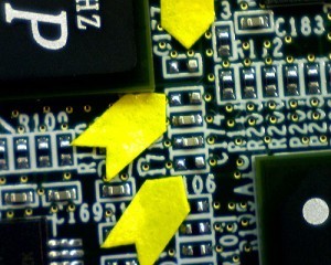
Corrosion due to Flux Residues
Flux is often used before soldering to reduce the oxides that are forming on the copper surface. However, the problem with this is that it can cause corrosion of the surface since it contains corrosive contents such as chlorine or bromine.
To get rid of these inorganic fluxes, the “no-clean” flux, which is composed of organic acids such as adipic or citric, was introduced. This kind of flux is being marketed as a no rinse flux, since organic acids decompose upon being subjected to temperature during the soldering process. Being a no-rinse flux, some manufactures do not bother to clean it.
This organic flux however may not decompose during a wave soldering process, resulting to a flux residue. Since the flux is being shielded from the molten solder, it may not reach the correct temperature for decomposition. This flux residue is still acidic in nature and is possible to cause corrosion in the area it was trapped.
Corrosion can be prevented by removing the flux residue as you clean the wave solder pallets. Use the same solvent that is used to dilute the flux and fiber-free cloths in cleaning the residue to avoid contaminating other products with debris.
Open Solder Joints
Open Solder Joints is caused by the lack of bond between the lead and the pack, or when there is solder only at the component lead but not on the circuit board. This results to an open connection on the PCB.
Other causes include the lack or inconsistency of solder paste or solder paste deposit, or the gap between circuit board pad and components leads. In addition, corrosion or contamination at component’s lead, weak solder paste and poor reflow profile may also cause it.
To prevent this defect, make sure you do the following during the PCB assembly stage: aspect ratio is correct, lead coplanarity is investigated and operator material handling procedures are monitored, extreme environmental effects are avoided, and PCB supplier’s fabrication issues are investigated.
Solder Joints Crack
Solder joints can develop cracks due to stress-induced factors over time. This crack may lead to fractures or the complete separation of the solder balls to the ball grid array, BGA. This results in displacement which causes the pin’s permanent failure and unwanted short circuits.
Experts examined trends in electronics during recent years that may lead to the cause of this defect. These trends include the use of lead-free solder and the use of compact BGA components.
Lead-free solder is known for higher brittleness and are more prone to cracks under stress than the traditional tin-lead solder. On the other hand, despite the advantages BGA possess, it is not very efficient at even distribution of stresses.
Both trends when combined increase the possibility of crack if it exceeds the maximum allowable stress. To avoid solder joints cracks, implement a strain Gage test on the PCB to make sure these trends are within the allowed stress limits. If it exceeded, rework or redesign the fixture to reduce stress to meet the required stress level.
Whether it is a cheap smartphone or complex machinery, defects in any form is a frustrating case. And in one way or another, these can be avoided if one is equipped with the proper knowledge and right skills.
With these problems in mind, Precision Tech assures its valued patrons that we have a deep understanding, knowledge and skills to prevent these defects. Expect only the most efficient, cost-effective and satisfying PCB assembly services that you deserve.